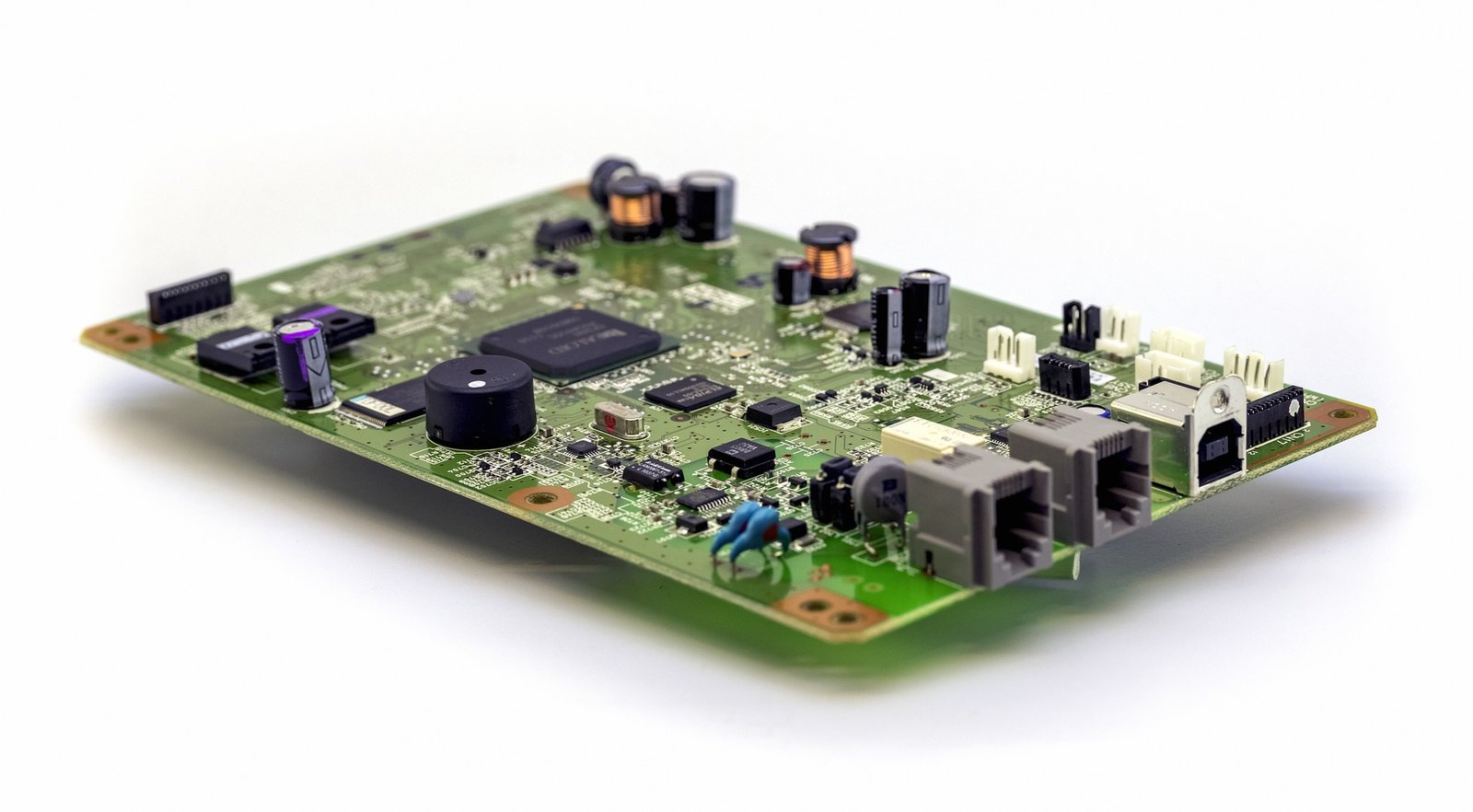
Multilayer PCB manufacturing methods include the plated-through hole (PTH) and high-density interconnect (HDI) methods, both achieved by combining different processes to realize the circuit board structure. Currently, the most widely used method is the PTH method, which has been developed and refined over more than half a century. The PTH method is mature in terms of equipment, materials, and processes, and has established a solid industrial foundation. It can be used to produce both double-sided and multilayer boards, with process and equipment reuse capabilities. In the PTH method, the insulating substrate surface and internal layer conductor patterns are interconnected through plated holes on the inner wall.
Taking the manufacturing process of a PCB factory as an example, the typical process flow for a rigid multilayer board is as follows:

Material Preparation:
PCB factories do not directly manufacture copper-clad laminates, prepreg sheets, or copper foils. Instead, these base materials are purchased from upstream material manufacturers. The base materials are typically standard large sizes, such as 1m x 1m or 1m x 1.2m. Before manufacturing, these materials are cut into sizes that fit the production line specifications.
Inner Layer Circuit Fabrication:
Multilayer boards typically use thin double-sided copper-clad laminates. After forming the inner layer circuits on the surface, the layers are laminated together.
A photosensitive dry film is applied to the double-sided copper-clad laminates for the inner layers. The film with the inner layer circuits is then attached and exposed to light.
After exposure, the boards are developed, and unwanted copper foil is etched away. After etching, the protective film that prevents etching of the circuits is removed.
Inspection and Brown Oxidation:
After the inner layers are formed, they undergo automatic optical inspection (AOI). Before lamination, to improve the adhesion between copper foil and the prepreg, a brown oxidation process is performed. The purposes of this process are:
· To increase the contact area between copper foil and resin, enhancing their bonding strength.
· To improve the wetting properties between the copper and the flowing resin, allowing the resin to fill any gaps and provide strong adhesion after hardening.
· To create a fine passivation layer on the copper surface to prevent the resin from reacting with the copper under high temperature and pressure, which could cause delamination.
Lamination:
The inner layers are stacked according to the designed layer structure, including the prepared inner layers, prepreg sheets, and outer copper foils, and then pressed together under heat to form a unified structure.
Drilling and Plating:
After lamination, interconnections between the layers are not yet formed, necessitating drilling followed by the deposition of a conductive copper layer on the hole walls to establish connections. The plating process includes three main steps: deburring, chemical copper deposition, and copper plating.
Chemical Copper Deposition and Full-Panel Electroplating
Chemical copper deposition involves using chemical methods to deposit a thin layer of copper on the insulated hole walls. Full-panel electroplating, on the other hand, increases the copper thickness on the conductive hole walls after the chemical copper deposition process. The process mainly includes three steps: desmearing, chemical copper deposition, and copper electroplating.
Desmearing clears resin smears in the holes while creating a slightly rough texture on the hole walls to enhance the adhesion between the copper and the resin. Chemical copper deposition forms a thin metallic layer on the hole walls, which serves as a seed layer for electroplating. Electroplating is used to increase the copper thickness on the hole walls. At this stage, the surface does not yet have circuit patterns, so this step is called “full-panel electroplating.”
Outer Layer Circuit Pattern
Objective: This process transfers the circuit pattern onto the copper-clad laminate.
Pattern Electroplating
Objective: Pattern electroplating is the process of electroplating a copper layer of the required thickness and a tin layer on the exposed copper traces or hole walls of the circuit pattern.
Resist Stripping
Objective: Using a NaOH solution to strip away the plating resist, exposing the non-circuit copper areas.
Etching
Objective: Etching involves using a chemical reaction to remove the copper layer from non-circuit areas.
Solder Mask
Comparison and Differences of Three Character Types
| Exposed Ultra-HD Characters | Stamped Characters | Screen-Printed Characters | |
| Actual Effect |  |  |  |
| Manufacturing Method | Manufactured using exposure machine | Manufactured using character stamping machine | Manufactured using silk-screen printing |
| Flatness | Very flat and smooth character surface, clear and neat | Character surface is not very flat | Character surface flatness is good |
| Contrast Sharpness | High accuracy of contrast | Contrast sharpness is moderate | Contrast sharpness has uniformity issues |
| Character Edges | Character edges are very smooth | Character edges are not smooth | Character edges are uneven and appear rough |
| Adhesion | Adhesion is relatively strong | Adhesion is moderate | Adhesion is good |
| Process Complexity | Complex process, higher cost | Relatively simple, higher cost | Traditional method, lower cost, hard to control quality |
The primary function of a PCB is to carry and connect electronic components. After pattern electroplating, areas that will not be contacted or soldered need to be protected with material to prevent damage or oxidation. Solder paste is typically used for component assembly, and the coating applied is referred to as the “solder mask.”
Legend
Objective: Legends are markings provided to make identification easier.
Surface Treatment
Unlike the solder mask process, surface treatment protects the areas that require soldering or contact, preventing the exposed copper foil from oxidizing due to air exposure, which could lead to poor soldering or contact issues.
Forming
Objective: Forming shapes the board according to customer specifications using die stamping or CNC routing. Forming methods include machine routing, punching, hand routing, and manual cutting. Note: CNC routing and punching offer high precision, hand routing is moderately precise, and manual cutting is less precise, limited to simple shapes.
Testing
Objective: Through electronic testing, defects such as open circuits or short circuits, which may affect functionality, are detected and identified.
Final Inspection
Objective: The final inspection checks for surface defects, and minor issues are repaired to prevent defective products from being shipped.
Reprinted from: Wu Chuanbin’s blog
*Arisentec is a leading PCBA manufacturer offering high-quality solutions for all your circuit board needs. With state-of-the-art facilities and a commitment to precision, Arisentec provides comprehensive services, from turnkey PCB assembly to flex PCB stiffener solutions. Whether you are looking for printed circuit board cost optimization or specialized products for automotive and smart home applications, Arisentec ensures top-tier results through advanced manufacturing techniques and exceptional customer service. Visit Arisentec’s website to explore their full range of offerings and elevate your PCBA projects to the next level.
-
![Manufacturing Process of Multilayer PCBs]()
Manufacturing Process of Multilayer PCBs
Multilayer PCB manufacturing methods include the plated-through hole (PTH) and high-density interconnect (HDI) methods, both achieved by combining different processes to realize the circuit board structure. Currently, the most widely used method is the PTH method, which has been developed and refined over more than half a century. The PTH method is mature in terms…
-
![Comprehensive Summary: 31 PCB Design and Routing Tips]()
Comprehensive Summary: 31 PCB Design and Routing Tips
When designing PCBs, routing is essential. The quality of the routing affects the aesthetics, production cost, circuit performance, heat dissipation, and device optimization. This article provides a comprehensive guide on PCB routing techniques: 1. The routing length should include the length of vias and solder pads. 2. The preferred routing angle is 135°. Arbitrary angles…
-
![Essential Files Required for PCB Fabrication]()
Essential Files Required for PCB Fabrication
In PCB fabrication, the transition from a digital design to a physical product involves several crucial steps. One of the most important phases in this process is the preparation and submission of the correct files. These files contain all the necessary information for manufacturing the printed circuit board to precise specifications. Below is an overview of…


The post Manufacturing Process of Multilayer PCBs appeared first on Leading PCB Manufacturer - Arisentec®.